News
Teach you if the noise performance of the power supply is sufficient?
- Author:ROGER
- Release on:2021-06-21
| From 5G to industrial applications, with collecting, delivery andstorageMore and more data is also expanding the simulationSignal processorThe performance limit of the pieces, some even gigabitate each second. Since the pace of innovation has never slowed down, the next generationelectronicThe solution will make the solution to further shrink,power supplyThe efficiency continues to improve and makes a higher requirement for noise performance. It may be considered to minimize or isolate energy domains (simulation, numbers, serial numbers, and digital input output (I / O)) The noise generated in order to achieve excellent dynamic performance, but pursue absolute minimum noise may reduce the revenue of the research. How does the designer know if the noise performance of the power supply is sufficient? First, quantify the sensitivity of the device, enabling the power spectrum output to match the power domain. Knowledge is power: save the excessive design to saveTimingThere is a great help to the design. This article outlines how to quantify the power supply noise sensitivity of the signal in the signal processing chain and how to calculate the maximum acceptable power supply. Also discussmeasuringSet. Finally, we will discuss some strategies that meet the demand of power domain sensitivity and real power supply noise. The subsequent article of this series will discuss how to optimize ADC, DAC andRF transceiverDistribution Network (PDN). Understand and quantify signal processing load sensitivity to power noise The first step in power optimization is to study the true sensitivity of the analog signal processing devices to power supply noise. These include the impact of the power supply noise on critical dynamic performance specifications, as well as the characterization of power supply noise - ie, power modulation ratio (PSMR) and power suppression ratio (PSRR). PSMR and PSRR indicate whether there is a good power suppression characteristic, but it is not enough to determine how low should be determined. This article describes how to determine the ripple band threshold or the maximum allowable power supply noise using the PSMR and PSRR. Optimized power supply system design is only possible to determine the threshold that matches the power spectrum output. If it is ensured that the power supply noise is lower than its maximum specification, the optimized power supply does not reduce the dynamic performance of each analog signal processing device. Impact of power supply noise on analog signal processing devices It should be understood that the effect of power supply noise on analog signal processing devices should be understood. These effects can be quantified by three measurement parameters:
Understanding the impact of power noise on these parameters is the first step in optimizing power noise specifications. No stray dynamic range (SFDR) Power supply noiseCouplingIn the carrier signal of any analog signal processing system. The impact of power supply noise depends on its intensity of carrier signals relative to the frequency domain. One measurement method is SFDR, which represents the smallest signal that can be distinguished from the big interference signal - specifically, the ratio of the amplitude of the carrier signal and the maximum spurious signal amplitude, no matter which position is in the spectrum, it has been obtained. Form formula: Carrier signal Spurious signal SFDR = no stray dynamic range (DB) Carrier signal = mean square root value (peak or full scale) of the carrier signal amplitude Spiration signal = mean square root value of the highest spur amplitude in the spectrum 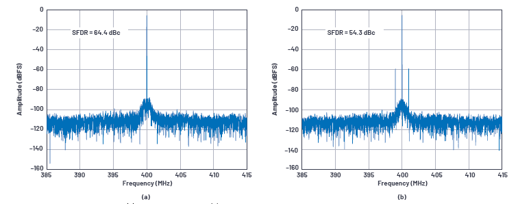 Figure 1. SFDR of the AD9208 high-speed ADC using (a) a clean power supply and (b) noise power supply. SFDR can be specified relative to full scale (DBFS) or carrier signal (DBC). Power ripple is coupled to carrier signals to generate interference spurious signals, which reduces SFDR. Figure 1 compares the SFDR performance of the AD9208 high-speed ADC in both cases of power supply and noise power supply. In this case, when 1 MHz power ripple is a rapid occurrence of ADC as a modulation spurFourierTransform (FFT) spectrum output carrierfrequencyAt the vicinity, power noise will reduce SFDR to about 10 dB. Signal ratio (SNR) SFDR depends on the highest spur in the spectrum, while the SNR depends on the total noise in the spectrum. The SNR limits the ability to identify low amplitude signals by the analog signal processing system, and theoretically affected by the converter resolution in the system. The SNR is defined as the sum of the sum of the carrier signal level and all noise spectrum components (except for the top five harmonics and DC), where: Carrier signal Spurious signal SNR = signal to noise ratio (DB) Carrier signal = mean square root value (peak or full scale) of carrier signals Spectrum noise = all noise spectrum components other than the top five harmonics and The noise power supply reduces the SNR by adding noise spectral components in the carrier signal to the output spectrum. As shown in FIG. 2, when a spectrum noise component is generated in the FFT output spectrum in the FFT output spectrum, the SNR of the AD9208 high-speed ADC is reduced from 56.8 DBFS to 51.7 DBFS. Phase noise (PN) Phase noise is parameters that measure signal frequency stability. Ideally,OscillatorA set of specific stable frequencies should be generated within a certain period of time. But in the real world, there are always some small interference amplitude and phase fluctuations in the signal. These phase fluctuations or jitter are distributed on both sides of the signal in the spectrum. Phase noise can be defined in a variety of ways. In this article, phase noise is defined as a single-sided tape (SSB) phase noise, which is a commonly defined definition that uses the power density of the carrier signal offset frequency and the total power of the carrier signal, wherein: Belt power density Carrier power SSB PN = Single Sideband Phase Noise (DBC / Hz) Sideband power density = noise power (W / Hz) per 1 Hz bandwidth under carrier signal offset frequency Carrier power = total carrier power (W) 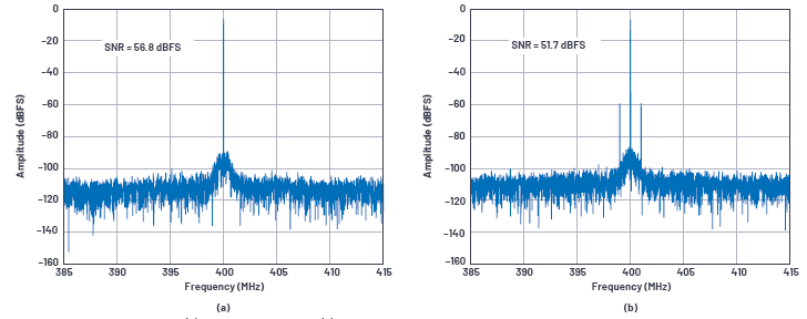 Figure 2. SnR of the AD9208 high-speed ADC using (a) Washing power and (b) noise power supply. 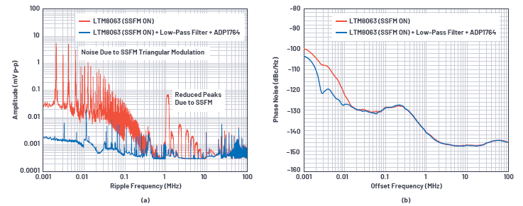 Figure 3. (a) Two different power supplies with significant differences in output noise. (b) When power is powered by these two power supplies, the phase noise performance produced by the ADRV9009 is. For analog signal processing devices, passclockThe voltage noise of the power supply voltage is coupled to the device clock generates phase noise, which in turn affects the frequency stability of internal vibration (LO). This expands the range of the LO frequency in the spectrum, increasing the power density at the offset frequency corresponding to the carrier, thereby increasing phase noise. Figure 3 compares phase noise performance of the ADRV9009 transceiver when power is powered by two different power supplies. Fig. 3A shows the noise spectrum of the two power supplies, and Fig. 3B shows the resulting phase noise. Both power supplies are based on LTM8063 μModule® with extension (SSFM)Stabilizer. The advantage of SSFM is thatBasebandDistributed within a certain range, improve the fundamental wave of the converterswitchFrequency and noise performance of its harmonics. From Figure 3A, this can be seen - note that there is a relatively wide noise peak at 1 MHz and its harmonics. It is necessary to trade out the consideration, the SSFM triangulation modulation frequency produces noise below 100 kHz - pay attention to the peak start from 2 kHz. Alternate power supply Add a low passfilterTo suppress noise above 1 MHz, add an ADP1764 low pressure difference (LDO) back regulator to reduce the wholeBottom noiseSound, especially the noise below 10 kHz (mainly the noise generated by SSFM). Due to additional filtering, the overall power supply noise is improved, thereby enhancing phase noise performance below 10 kHz offset frequency, as shown in Figure 3B. Power noise sensitivity of analog signal processing devices The sensitivity of the load on the power ripple can be quantified by two parameters:
Power Suppression ratio (PSRR) PSRR represents the ability of the device to attenuate the power pin noise within a certain frequency range. Typically, there are two types of PSRR: static (DC) PSRR and dynamic (AC) PSRR. DC PSRR is used to measure the output offset change caused by the change in DC power supply voltage. This is almost no attention, because the power system should provide a stable adjustment of DC voltage to the load. On the other hand, the AC PSRR represents the ability of the device to suppress AC signals in the DC power source within a certain frequency range. The AC PSRR is determined by injecting a sine wave signal in the power pins of the device, and observing the error pseudo dispersible on the data converter / transceiver output spectrum in the injection frequency (Fig. 4). AC PSRR defines the ratio of the corresponding error stray amplitude and output spectrum, where the measured injection signal amplitude is: Inject ripple Error spur Error Dispersions = Spirus Amplitude in Output Spectroscopy caused by injecting ripple Injection ripple = sine wave amplitude coupling and measured at the input power pin 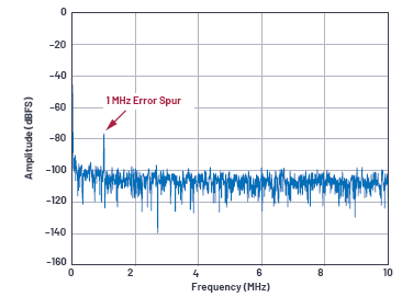 Figure 4. Error spurs in the analog signal processing device output spectrum caused by power ripple. Figure 5 is a block diagram showing a typical PSRR setting. Taking the AD921310 GSPS high speed ADC as an example, there is a source coupled 1 MHz, 13.3 mV peaks on the 1.0 V analog power rail. The corresponding 1 MHz digitized spur were found on the ADC-108 DBFS FFT spectrum. 1 MHz digitized pseudo is -81 dBFS, the corresponding peak voltage is 124.8 μV, and the simulation input of the 1.4 V peak value is fully gradable. 1 MHz of AC PSRR was calculated using Equation 4 to give 1 MHz AC PSRR to 40.5 dB. Figure 6 shows the AD9213 1.0 V AVDD rail exchange PSRR. 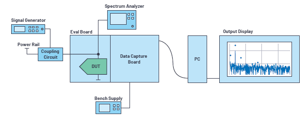 Figure 5. PSRR / PSMRtestSet up simplified block diagram. 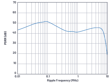 Figure 6.1.0 V AVDD rail AD9213 high speed ADC AC PSRR. Power modulation ratio (PSMR) The impact of PSMR on analog signal processing devices is different from PSRR. PSMR is usedRFWhen the carrier signal is modulated, the device is sensitive to power supply noise. This effect can be considered as a modulated stranded surrounding the carrier frequency applied to the device, exhibiting the carrier sideband. Power modulation by using line injector / couplingCircuitThe input ripple signal is combined with a clean DC voltage. Power ripple is injected into the power pin from the signal generator as a sine wave signal. The sine wave modulated to the RF carrier generates the sideband strap, its offset frequency is equal to the sinusoidal wave frequency. The impact level is affected by the amplitude of the sine wave and the sensitivity of the device. The simplified PSMR test setting is the same as PSRR, as shown in Figure 5, but the output mainly displays the carrier frequency and its edge strip, as shown in FIG. PSMR is defined as the ratio of the power injection ripple amplitude and the carrier surrounding the splice amplitude, wherein: Inject ripple Modulation spur Modulation spurious = strapless magnitude of the carrier frequency edge caused by injection ripple Injection ripple = sine wave amplitude coupling and measured at the input power pin 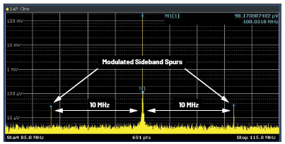 Figure 7. Modulation sideband spur in carrier signals caused by power ripples. Assuming the AD917512.6 GSPS high-speed DAC works at 100 MHz carrier, and there is a 10 MHz power ripple of 3.05 mV peaks in the 1.0 V AVDD rail. The corresponding 24.6 μV peak-to-peak modulation stray, the offset frequency is equal to about 10 MHz, which is equal to about 10 MHz. 10 MHz PSMR was calculated using Equation 5 to obtain 41.9 dB. Figure 8 shows the channel DAC0 AD9175 1.0V AVDD rail PSMR at various carrier frequencies. 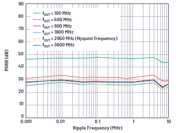 Figure 8.1.0 V AVDD rail (channel DAC0) AD9175 high speed DAC PSMR. Determine the maximum allowable power ripple The PSMR can be combined with the reference threshold of the power receiving device to determine the maximum allowable voltage ripple of each power domain of the analog signal processing device. The reference threshold itself can be one of several values, representing the device tolerance without significantly affecting its dynamic performance (caused by power ripple). This strapless level can be a percentage of no stray dynamic range (SFDR), the lowest significant bit (LSB) or output spectrum. Equation 6 shows that the maximum allowable input ripple (VR_max) is functional relationship with the psmr and the respective devices, wherein: Threshold VR_max = maximum allowable voltage ripple on each of the power rails before the output spectrum is generated in the noise of output spectrum PSMR = Noise sensitivity (DB) of the target power rail (DB) Threshold = predefined reference threshold (output spectrum is noise in this article) For example, the output spectrum of the AD9175 is about 1 μV peak value. The PSMR of 1800 MHz carriers was about 20.9 dB under 10 MHz ripple. Using Equation 6, the maximum allowable ripple of its dynamic performance is 11.1 μV peak value in the device power pins. Figure 9 shows a combination of the maximum allowable ripple of the AD9175 1.0 V AVDD rail to the LT8650S buck SILENT SWITCHER® regulator (band and non-output LC filter). The regulator spectrum output contains a spurious scatter in the base wave switching frequency and its harmonics. LT8650s powered directly for the AD9175 generates a base frequency that exceeds the maximum allowable threshold, resulting in a modulated edge strap spurray in the output spectrum, as shown in FIG. Simply adding an LC filter to the maximum allowable ripple, as shown in Figure 11. 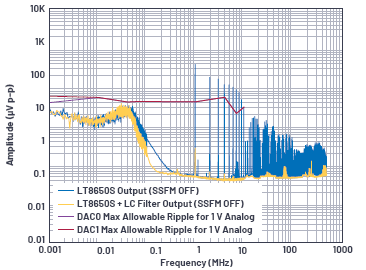 Figure 9. The relationship between the power spectrum output and maximum allowable voltage ripple on the 1.0 V AVDD rail.  Figure 10. AD9175 DAC0 output spectrum at 1800 MHz carrier frequencies (directly output to the AVDD rail using the LT8650S DC-DC Silent Switcher converter). 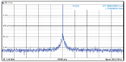 Figure 11. AD9175 DAC0 output spectrum at 1800 MHz carrier frequencies (using LT8650s with LC filter power). in conclusion Excellent dynamic performance of high-speed simulation signal processing devices is easily weakened by power supply noise.In order to avoid the decrease in system performance, it is necessary to fully understand the sensitivity of the signal link to the power supply noise.This can be determined by setting the maximum allowable ripple, the maximum allowed ripple is critical to the distribution network (PDN) design.After knowing the maximum allowable ripple threshold, you can use a variety of ways to design optimize the power.If the maximum allowable ripple has a good margin, the PDN does not reduce the dynamic performance of the high-speed analog signal processing device. |