News
New Products | China's first compatible optical coupling DESAT protection function IGBT / SIC Isolation Drive SLMI33X
- Author:ROGER
- Release on:2021-07-20
Silumin semiconductor as a one-stop provider of domestic drive type ICs, continued to deep till isolation drive, and officially released the first single-channel with DESAT protection in China recently.IGBT/ SIC Isolation Drive SLMi33X. SLMI33X built-in fast-saturation (DESAT) fault detection function, Miller clamp function, drain open fault feedback, soft shutoff function, and selectable self-recovery mode, compatibleOptocouplerIsolation drives provide high quality, high-performance alternatives to customer engineers. By adopting industry-leading doublecapacitanceIsolation technology and "OOK" transmission technology, SLMI33X implemented 5KVRThe Isolation voltage of the MS and the isolation voltage of up to 10 kV, and has a common mode transient immunity of more than 100 kV / US (min.) (cmTi), Satisfying SiC power devices pair CMTiHigh requirements guarantee reliability and stability in extreme harsh working conditions. The DESAT threshold of the SLMI33X is 6.5V or 9V, the maximum driverCurrentThere are 1.5A, 2.5A and 4.0A three gears, which can be widely used in motor drive, high powerInverter, Uninterruptible power supply (UPS), EV charging,InverterEquisical application scenarios.
SLMI33X performance advantages
- Anti-negative capacity
- Maximum delay is shorter
- The voltage range on the input side and the output side is wider
- CmTiHigher value, better anti-interference ability
Typical application of SLMI33X in IGBT three-phase bridgeCircuitAs shown in Figure 1. When working properly, the ANODE and Cathode receive the control signal of the controller, and the VOUT outputs the drive signal to drive the IGBT's opening and shutdown. BeShort circuitWhen the protection, the IGBT's VCE voltage is detected by DESAT. When the voltage on the DESAT is higher than 6.5V or 9.0V, it turns off the VOUT output and transmitted to the control terminal side and pulls the FAULT.
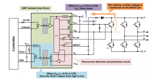
Figure 1. SLMI33X typical application circuit diagram SLMI33X pin definition and package is shown in Figure 2, which is encapsulated into SOIC 16 wide body, and provides a climbing and gap distance greater than 8 mm.
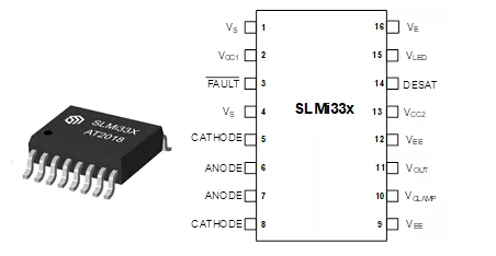
Figure 2. SLMI33X pin definition and package current SLMI33X has passed customers in different fields such as various major inverters, inverterstestThere are 12 series of products to choose from, please email the samples to [email protected].
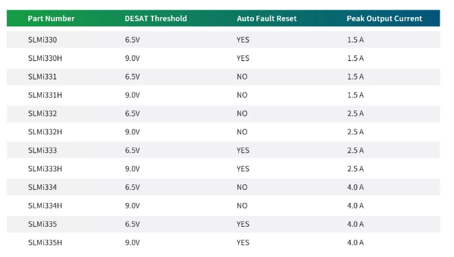
Figure 3. SLMI33X Guide